Architecture
The architecture we had in mind for our project consists in a single transmitter and multiple receivers. Every receiver has its unique ID, in this way the firmware is able to understand if it needs to be updated with the price contained in the packet received or if the packet has to be discarded. We also assumed that the transmitting side has a database containing all the prices and corresponding IDs so the information contained in the receivers is periodically refreshed as a form of error correctionTransmission-side Schematic

The transmission side schematic is quite simple: the output pin of Arduino chosen in the transmission firmware is connected to an LED with a series resistor sized properly to guarantee that the light produced has enough intensity to be properly received and interpreted at a reasonable distance. The maximum voltage output of the Arduino Due is 3.3V so we used a 150 Ohm resistor resulting in a current of about 20 mA.
The main thing which requires attention is the frequency of the PWM signal coming from the output pin: if the frequency isn't high enough there could be some flickering in the light emitted by the LED. In this project we employed a minimum frequency of 250Hz and so we managed to avoid any flickering.
Reception-side Schematic
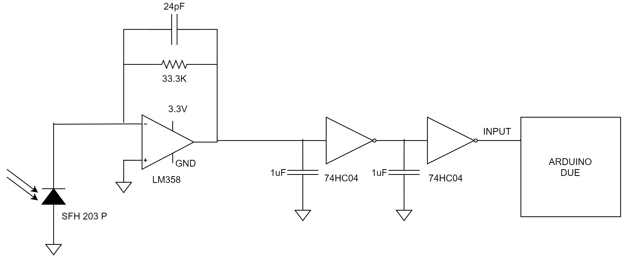
In the reception side schematic things get a bit more tricky. The idea is to convert the current generated by the photodiode, which is hit by the light produced by the transmitter, into a signal which can be in turn interpreted and elaborated by the Arduino Due to be then shown on the serial monitor. In order to achieve this, the first stage of the schematic must be the current-to-voltage converter. We used an online tool developed by Analog Devices (which can be found here) where we inserted our photodiode model, our supply voltage and the wanted bandwidth. The supply voltage is 3.3V as we can't exceed that value otherwise we could damage the pins of the Arduino and the wanted bandwidth we set is 10kHz which we thought the best compromise between the operating specifics of our transmitter and the GBW of the OpAmp we used.
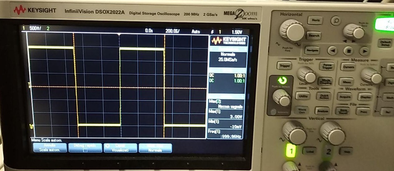
At first we tried connecting the output of the converter directly to the input pin of Arduino but we soon found out that the internal circuitry wasn't able to properly detect the edges of the signal resulting in a wrong total count in our interrupt routine. In the image below there is a comparison between our signal and the one outputted by a waveform generator, it can be clearly seen that our edge isn't as sharp as it is needed to be for a proper reading

So to fix this issue we tried to transform our signal into a more "digital" shape, meaning we tried to give the signal faster rising and falling times. By doing this we ensured the noise wasn't able to destroy the reading of the signal especially in the proximity of the logic threshold used by Arduino. This step was achieved by using logical inverters put in series: the switch from high to low output (and viceversa) was considerably faster and less prone to noise influence. We also added capacitors to the input of each inverter to remove high frequency noise that could damage the reading. Below is the waveform after our fixes