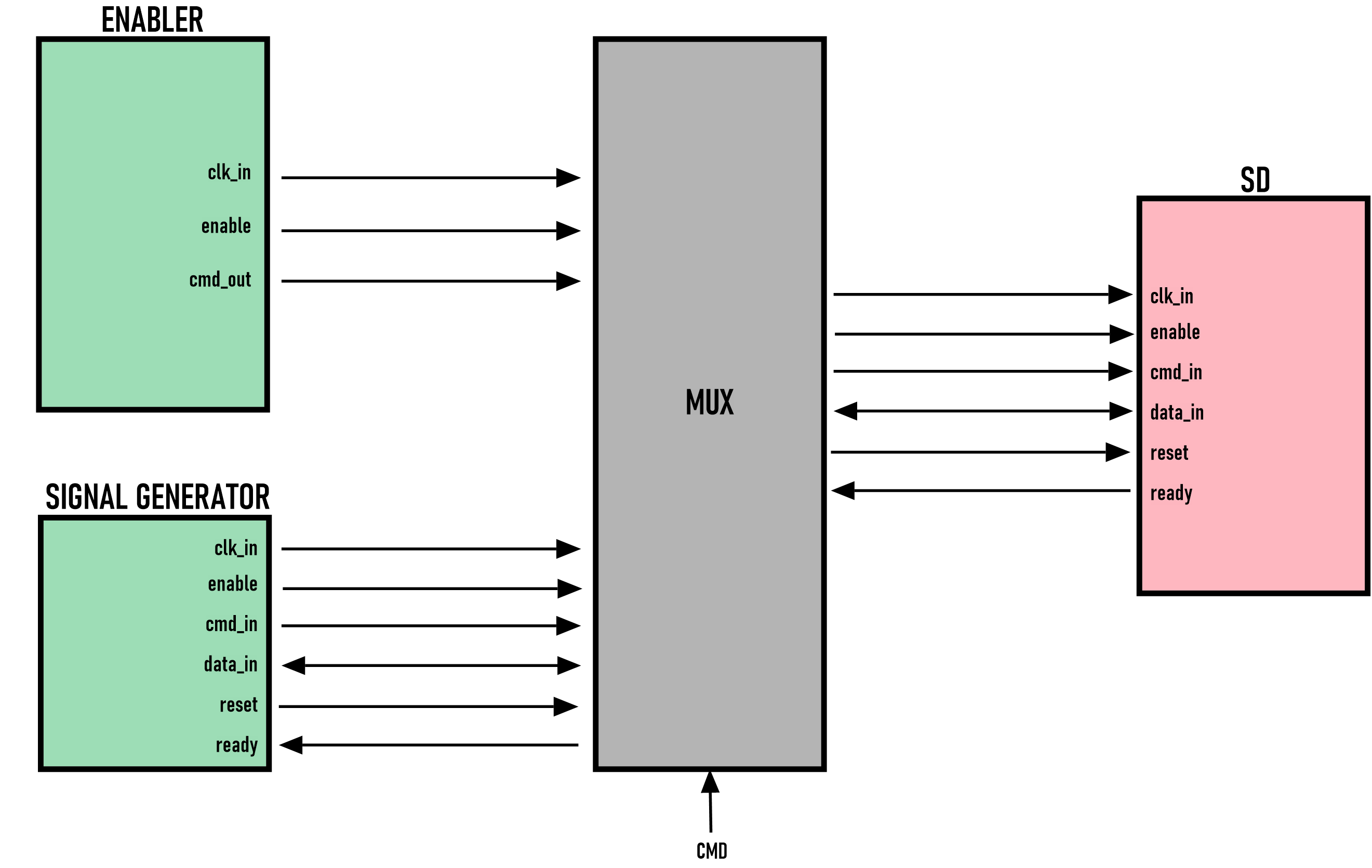
Interface and memory
The interface is a component which manages the master output signals (SD card input signals) to adapt them to the memory input signals.
It is composed by six signals which interface with the external world and other six signals which connect it to the memory component.
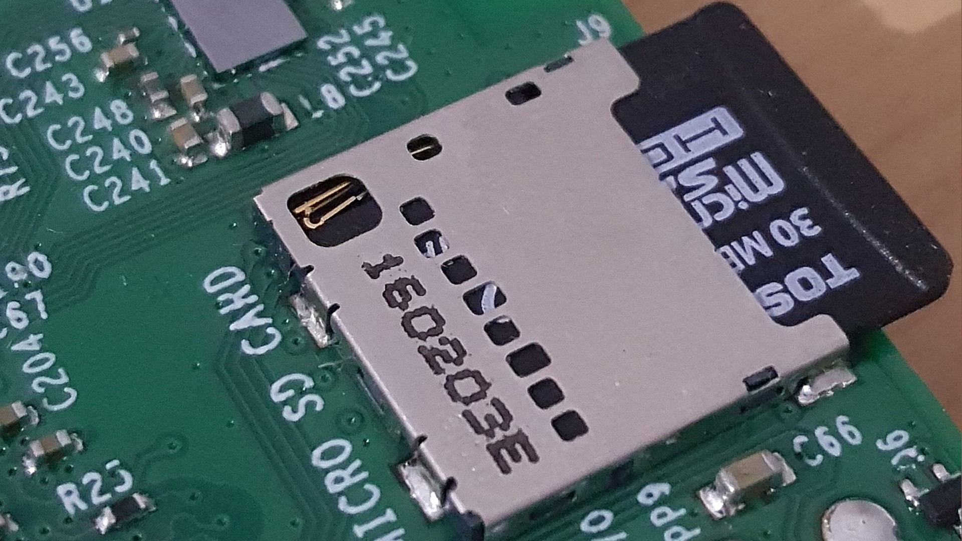
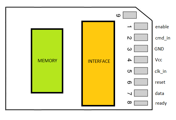
The prototype card pin layout is composed by the following listed signals. They are all of std_logic type and thus 1-bit long signals. The following list does not include
the power pins, which are shown in the picture below.
- clk_in : it represents the input clock of the card.
- enable: if set to high, it enables the input signal elaboration.
- cmd_in: it allows the master to send the read/write command and the hidden memory enabling command by the enabler device.
- data: serial bus which contains the data bits which have to be saved due to a write operation or have been read from memory after a read operation. Thus it is a signal that can be used in both
directions (inwise and outwise) according to the performed operation.
- ready: if set to high, it indicates that the performed operation had reached its end.
- reset: signal that re-boots the card.
The following image shows the chosen position of the different pins in relation with the physical contact structure of a SD adaptor.
Once the card is inserted into the hosting device (master), some preliminary actions are performed. After that, the card goes into a waiting state and listens for a known command:
The previous three actions are performed in a cuncurrent manner. In the first one (Flag reading to understand if the hidden area is enabled), the card understands whether its usage
in the hidden area is enabled or not by reading a special memory cell in which a single bit is stored. If that bit is high, the hidden memory partition is enabled. That value is copied
in a card internal flag for a future usage during a read/write operation. On the other hand, the special memory cell content is set to 0 so that, in case of the card reboot, the hidden
memory partition will be disabled. To enable that section again, the user must connect the card to the enabler device and then put it back on the master device.
The second phasee (Signal recieving FSM enable) initiate to an idle state the FSM which understands the input commands given by the master device. In this state, the card waits for
the enable signal going up to indicate that an action can start and a new command is given as input.
The third phase understands if the card is connected to an enabler device when it boots up. If that is correct, the enabler device is recognised and the flag representing the hidden
partition enable is set to high for a future use.
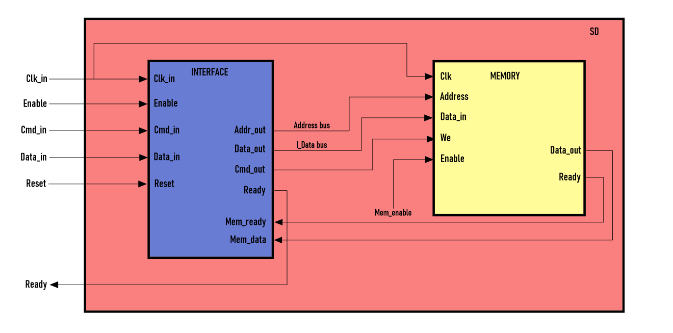
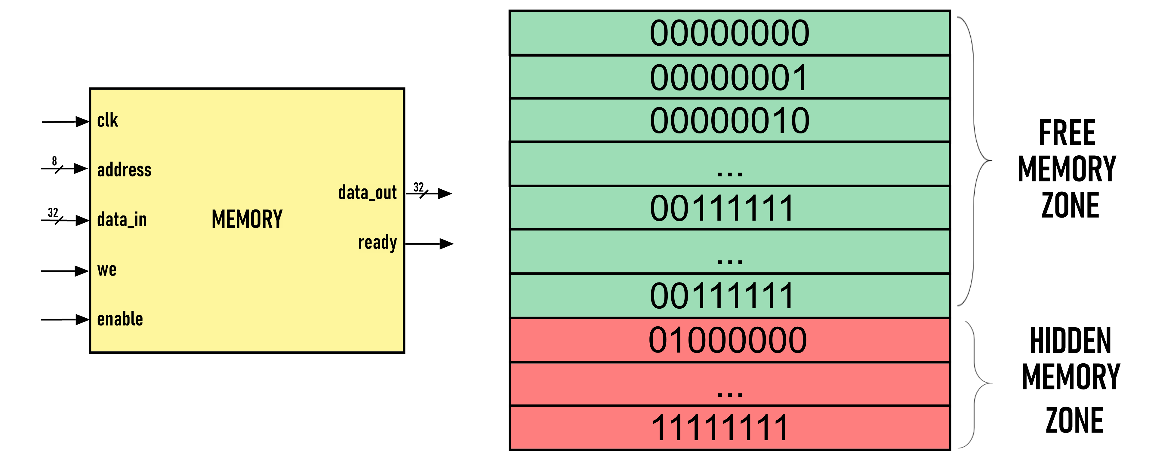
Memory
The memory zone is divided into two sections: a visible one, which is usable by everyone who wants to use the SD card, and a hidden partition which is accessible only after the SD card has been enabled.
The enabling operation can be done by inserting the card into the enabler device. Usually, SD cards are endowed with a non-volatile flash memory to store data. In this project, the afromentioned memory is simulated
with a RAM memory composed by 256 words each of them is 32 bit long. The data persistency is realized by saving the whole memory content on a text file after every write operation. A 8-bit long address can be used
to address the memory where the two most significant bits could be forced to 0 in case the SD card is not enabled to work in the hidden zone.
A general memory structure scheme is provided in the following image:
Talking about VHDL sythesis, the memory block is endowed with five input signals and two output signals. The address signal is a 8-bit bus whereas data_in is a 32-bit long bus. Once the memory has performed
an operation, it sets to high the ready signal in oreder to indicate the end of the operation. In case of a reading operation, the obtained data are put on the data_out signal, which is a 32-bit bus.
Insidewise, to simulate data persistency, the whole memory content is stored in a text file at each end of a write operation. That file is used every time the SD is booting up to upload the last state of the memory.
Interface
As mentioned above, the working principle of the interface and thus of the whole system, is based on a finite state machine (FSM) which has to comprehend and translate every command that comes from the master device.
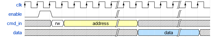
According to the operation that the system has to perform, the input commands have to follow a communication protocol which describes how to put information on the card input signals.
The chosen protocol realizes a simplified version of the SPI protocol used to interface with a flash memory found on the majority of the non-volatile memory based devices.
The working priciple of our protocol needs three signals:
- enable : it is set to logic high when a new command has to be given.
- cmd_in: it is used to insert the instruction (read/write) and the memory address in which the operation has to be performed.
- data: it is used to insert/retrieve data to write/read onto the memory at the specified address.
The signals behaviour in this phase is the following:
Once enable is high, on cmd_in the communication of the command to execute starts by inserting a bit which tells the system whether it's a write or read operation. After that, the memory address bits are
inserted in a serial manner. In case of a write action, after the memory address has been put on the cmd_in signal, the data bits can be inserted serially on data signal.
The address and data that has to be saved on memory bits have to be put as input to the memory block, which means that the interface has to deserialize those bit using a SIPO register. The obtained parallel data stream will be inserted on the address and data_in signals.
If the hidden memory zone access flag is set to 0, the two most significant bits of the memory address in which the specified action has to be performed are set to 0 before giving that memory address as input to the memory block.
In this way, the SD card must work only on the free-access zone without letting anyone access to the hidden memory addresses. The user won't notice anything strange because the specified operation will be done in a different address on the clear zone.
The following image better explains this principle. In fact, the user wants to perform a write opration followed by a read operation on the same memory address which is contained in the hidden zone. Because the hidden partition has not been enabled yet, that address is changed and the operation is performed on the clear zone. From an
outside point of view, the data seems to be stored in the provided address.
In case of a read action, the output data bits (a 32-bit long string found in the specified address) will be given on data_out signal. To do so, the interface has to serialize the data which comes from memory using a PISO reister and put them on the data signal.
The SD card user has indeed to use the data signal both in an input and output way according to the performed action.
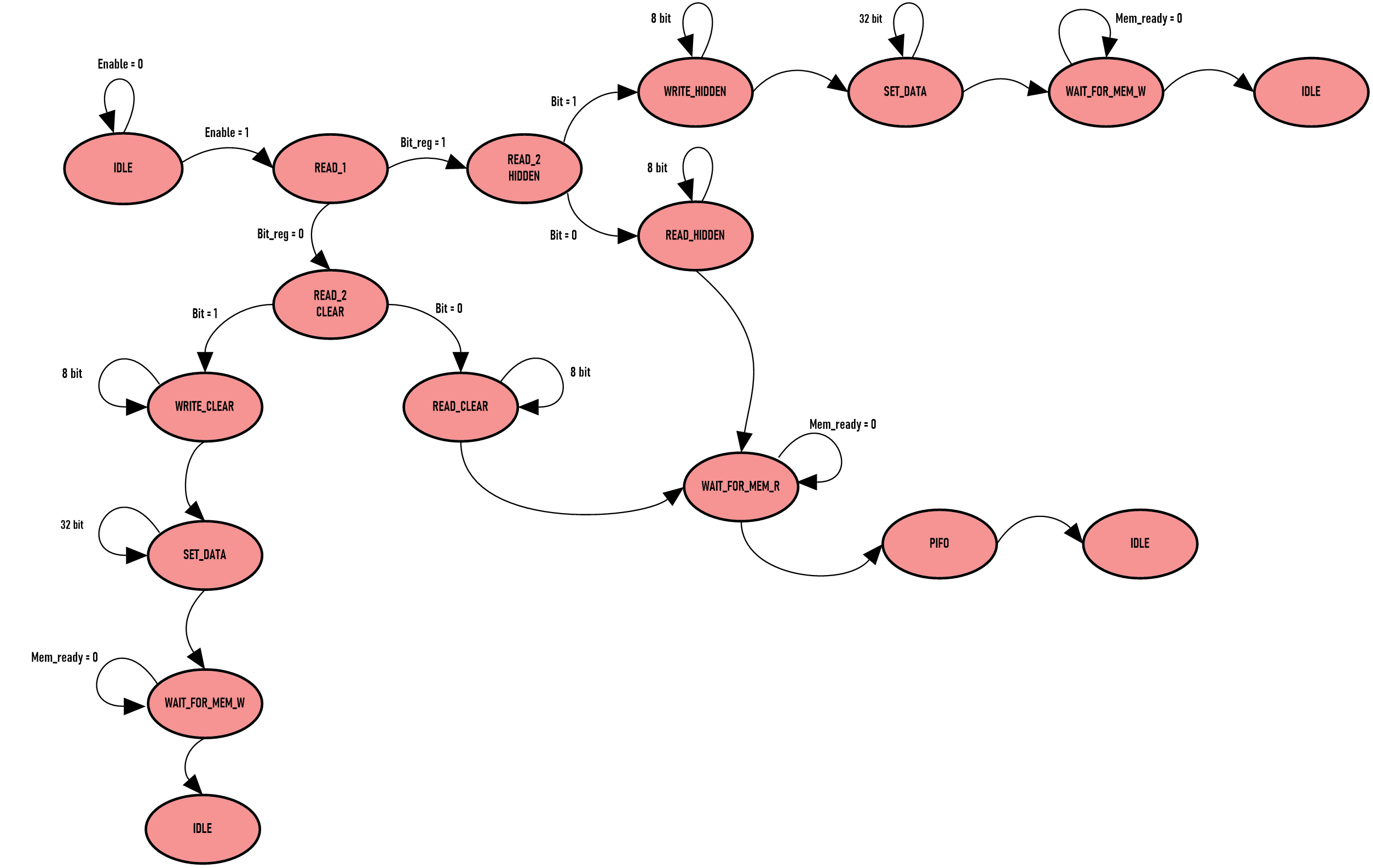
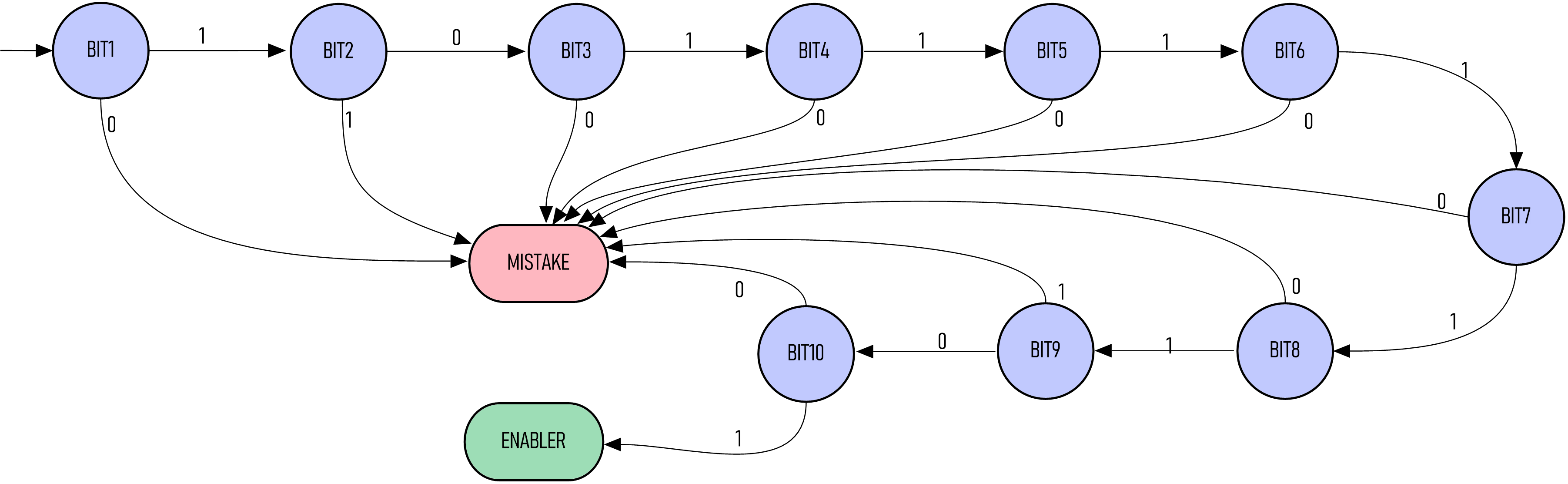
All the afromentioned operation can be descibed with the following FSM:
This FSM is composed by 17 states where the IDLE state is its root. In that state the device is in a waiting period listening for a specified action to do. As soon as the enable signal goes high, the elaboration will start. Every state performs its own precise operations.
The first part of the FSM concentrates on the undestanding of the provided command and on the reading of the hidden partition enabling falg. This is made to understand whether the hidden partition has to be visible or not. The following table shows how an operation is understood
in function of the signal values:
| reg_enable |
cmd_in (r/w) |
actions to perform |
final state |
| 1 |
1 |
Write action with enabled hidden zone |
WRITE_HIDDEN |
| 1 |
0 |
Read action with enabled hidden zone |
READ_HIDDEN |
| 0 |
1 |
Write action with NOT enabled hidden zone |
WRITE_CLEAR |
| 0 |
0 |
Read action with NOT enabled hidden zone |
READ_CLEAR |
On the final states, the address in which to perform the indicated action is read. That address is then put on a 8-bit long signal which interfaces itself with the memory block. In case of a write operation
the next state will be SET_DATA, in which the 32 bits of the data that has to be written are read and put on a same-lenght bus. At this point, the evolution of the FSM goes to WAIT_FOR_MEMORY_W, where the memory is enabled to perform
the writing. The interface block listens on the ready signal from the memory to indicate that the action has been correctly completed. Once that signal goes high, the interface goes back to the IDLE state and waits for another command.
On the other hand, in case of a read operation, from the final states, the FSM goes to WAIT_FOR_MEM_R in which it waits for an output from the memory block to be put on the output bus. At this point the execution proceeds on the PISO state. This state serializes
the data obtained from memory and put bit by bit on the data pin of the card. As it happend in the write opration, the FSM then goes to the IDLE state.


 SD.vhd